Where Can You Learn More About Advanced Printed Circuit Technology?
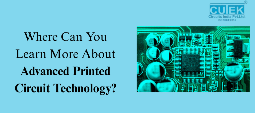
Advanced Printed Circuit Technology is the backbone of today’s high-performance electronic systems. From smartphones and medical devices to automotive electronics and aerospace systems, modern innovations depend on efficient, miniaturized, and high-density PCB designs.Companies like Cutek, known for precision PCB manufacturing and reliable engineering processes, play a major role in supporting this advancement. If you want to build a strong foundation in this domain, you need the right learning sources—online, offline, industry-based, and hands-on. What Is Advanced Printed Circuit Technology? Advanced Printed Circuit Technology includes highly specialized PCB processes used by leading manufacturers like Cutek.It covers: HDI (High-Density Interconnect) PCBs Flexible & Rigid-Flex PCBs Microvia & Blind/Buried VIA Technology Impedance-Controlled Designs High-Frequency RF & Microwave PCBs Advanced Materials (Rogers, Taconic, PTFE, Polyimide) Companies such as Cutek use these technologies to create compact, durable, and high-performance circuit boards for complex electronic applications. Why Should You Learn Advanced Printed Circuit Technology? Career Advancement Industries like telecom, EVs, aerospace, defence, and consumer electronics depend on companies like Cutek that manufacture advanced PCBs. Learning this technology increases your chances of working with leading organizations. Better Design Quality When you understand how manufacturers like Cutek build HDI and high-speed PCBs, you naturally design better products with fewer errors. Competitive Edge The electronics industry is rapidly shifting toward miniaturization, flexible designs, and high-speed applications. Skills in advanced PCB technology—used by companies like Cutek—give you an edge in the job market. Where Can You Learn Advanced Printed Circuit Technology Online? Online Courses Coursera & Udemy IPC Online Training Altium Academy Manufacturer Webinars(Many PCB manufacturers, including Cutek, share guides, resources, and documentation useful for advanced learning.) Free Learning Resources YouTube channels (Altium, EEVblog, HashDefine) PCB design blogs, engineering tutorials High-speed design articles Manufacturer design guides(Cutek’s documentation can help you understand real fabrication capabilities and advanced stack-up structures.) What Offline Sources Can Help You Learn? Engineering Colleges & Institutes Electronics engineering courses cover fundamentals that prepare you for advanced PCB design. IPC Certification Programs Globally recognized and aligned with industry standards followed by manufacturers like Cutek. Workshops & Industrial Training Visiting PCB manufacturers such as Cutek helps you understand fabrication, testing, assembly, and DFM processes in real-world environments. Electronics Expos Events like Electronica, PCB West, and productronica give exposure to advanced technologies used by companies across the world, including players like Cutek. Which Tools Should You Learn for Advanced Printed Circuit Technology? Design Software Altium Designer Cadence Allegro Mentor Graphics KiCad Eagle OrCAD Simulation Tools Signal Integrity (SI) Power Integrity (PI) Thermal Analysis EMI/EMC Simulation Learning these tools helps you design PCBs compatible with advanced manufacturing processes used by companies like Cutek. How Do Professionals Stay Updated? Industry Publications IEEE Journals PCB Design Magazine SMT Today Manufacturer Updates Companies like Cutek, Rogers, Isola, and AT&S regularly share updates on materials, stack-ups, manufacturing limitations, and industry trends. Online Communities Reddit r/PCB StackExchange Electronics Altium CommunityThese platforms help learners stay updated with techniques used by professional PCB companies like Cutek. Frequently Asked Questions (FAQ) 1 . Is Advanced PCB Technology Hard to Learn? Not difficult—consistent practice and exposure to real manufacturing examples (for example, Cutek’s PCB capabilities) make learning smooth. 2 .How Long Does It Take to Learn Advanced PCB Design? Typically 3–6 months, depending on your practice, tools, and understanding of real fabrication rules used by companies like Cutek. 3. Do I Need Expensive Tools to Learn PCB Design? No. Start with KiCad. As you progress, you can move to professional tools used by PCB manufacturers like Cutek. 4. Are Certifications Important? Yes. Certifications like IPC improve credibility and align with the quality standards followed by advanced PCB companies. Contact Cutek Circuits Address: 4/4 Badhe Industrial Estate, Next To Silver Star Hall, OPP. To Angaraj Hotel, Kondhwa, Pune, Maharashtra 411048, INDIA Phone: +91 92255 24304 | +91 98237 84304 | +91 87930 34304 Email: info@cutekcircuits.com | sales@cutekcircuits.com Website: https://cutekcircuits.com
How to Optimize the Flexible PCB Manufacturing Process
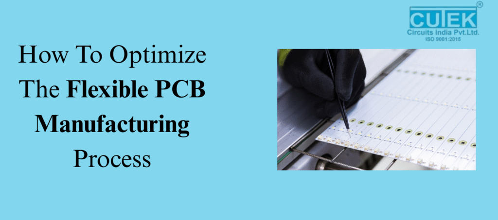
Flexible PCB manufacturing plays a vital role in today’s compact, lightweight, and high-performance electronic devices. Industries like wearables, automotive, aerospace, and medical electronics depend on flexible circuits for improved design freedom and durability.Optimizing the Flexible PCB manufacturing process not only ensures higher quality but also reduces waste, minimizes errors, and boosts long-term reliability.Below, we explore the most important questions that help manufacturers streamline and improve the entire process. What Factors Influence Material Selection in Flexible PCB Manufacturing? Material selection is the foundation of an optimized Flexible PCB manufacturing process. Choosing the right polyimide films, copper foils, and adhesives greatly influences circuit flexibility, heat resistance, and overall durability.High-grade materials ensure the PCB can bend repeatedly without cracking or losing conductivity. Low-quality materials may reduce cost initially but often lead to failures during thermal or mechanical stress. How Does Good Circuit Design Improve Manufacturing Efficiency? An optimized circuit design reduces stress on bend areas and prevents long-term damage. Techniques like rounded trace corners, even trace width, proper spacing, and avoiding vias in flex zones significantly improve performance.A well-designed layout also lowers the risk of delamination, increases signal integrity, and ensures smoother fabrication with fewer design reworks. Why Is Precision Etching Critical for Flexible PCB Quality? Etching defines the conductive pathways on a flex PCB. Inaccurate etching—whether too much or too little—weakens the copper traces and creates potential short circuits.Using controlled chemical etching and high-resolution imaging ensures sharp, accurate, and uniform trace formation. This leads to higher reliability and reduces the chances of defects during final product testing. How Do Drilling and Plating Impact Flex PCB Performance? Drilling and plating determine how well electrical connections are formed between layers. Laser drilling offers higher accuracy for micro-vias used in modern electronic devices.Clean, smooth hole walls allow efficient plating, ensuring even copper thickness and strong electrical paths. Proper plating also enhances mechanical resilience during bending and flexing. What Role Does Coverlay Application Play in PCB Durability? Coverlays serve as protective layers that shield circuits from moisture, heat, and mechanical abrasion. Incorrect lamination can cause wrinkles, air gaps, or misalignment, which leads to circuit failure.Optimized coverlay lamination ensures a smooth, bubble-free finish, improving the PCB’s ability to withstand continuous flexing without damage. How Does Automation Enhance Flexible PCB Manufacturing? Automation minimizes human error and ensures consistent results at every production stage. Automated tools for imaging, alignment, inspection, and lamination offer higher precision and reduce cycle times.Automated systems also help in tracking defects early, keeping overall quality stable, and cutting down production costs. Which Quality Control Methods Ensure High Manufacturing Standards? Quality control is essential for identifying defects before the PCB moves to final assembly. Effective methods include: Automated Optical Inspection (AOI) – Detects trace defects and misalignment Electrical Testing – Ensures proper signal flow Thermal Stress Testing – Checks heat resistance Mechanical Flex Testing – Ensures durability during repeated bending These steps guarantee that every flexible PCB meets industry performance standards. What Strategies Help Reduce Costs Without Compromising Quality? Cost optimization focuses on intelligent production planning, not cutting essential quality steps.Key strategies include: Using efficient panel layouts Reducing unnecessary layers Standardizing trace widths and spacing Selecting cost-effective yet high-quality materials These methods help manufacturers achieve better output at lower production costs. Optimizing the Flexible PCB manufacturing process requires attention to design, materials, precision, automation, and thorough quality control. By following these best practices, manufacturers can create flexible PCBs that are reliable, long-lasting, and cost-effective—meeting the demands of today’s advanced electronics industry. FAQs 1. What is Flexible PCB manufacturing? It’s the process of making bendable circuit boards used in compact and flexible electronic devices. 2. Why is optimizing the process important? It improves quality, reduces defects, increases efficiency, and lowers production costs. 3. What materials are best for Flexible PCBs? Polyimide films, flexible copper foils, and strong adhesives offer the best flexibility and durability. 4. How does good PCB design help? Proper trace routing and avoiding stress points improve performance and extend PCB life. Contact Cutek Circuits Address: 4/4 Badhe Industrial Estate, Next To Silver Star Hall, OPP. To Angaraj Hotel, Kondhwa, Pune, Maharashtra 411048, INDIA Phone: +91 92255 24304 | +91 98237 84304 | +91 87930 34304 Email: info@cutekcircuits.com | sales@cutekcircuits.com Website: https://cutekcircuits.com