PCB designing and flexible PCB manufacturing are core strengths at Cutek Circuits. We are one of the most trusted PCB design companies in India, delivering end-to-end solutions based on advanced printed circuit technology for unmatched performance, reliability, and manufacturability.
Our expert team crafts robust PCB layouts for a wide range of applications, including industrial automation, medical electronics, consumer appliances, automotive systems, and defense technologies.
Whether it’s a simple single-layer board or a complex, high-density multilayer design, our PCB designing services are customized to meet your specific needs. We focus on signal integrity, thermal performance, and cost-effective manufacturing to ensure your product achieves both technical and commercial success.
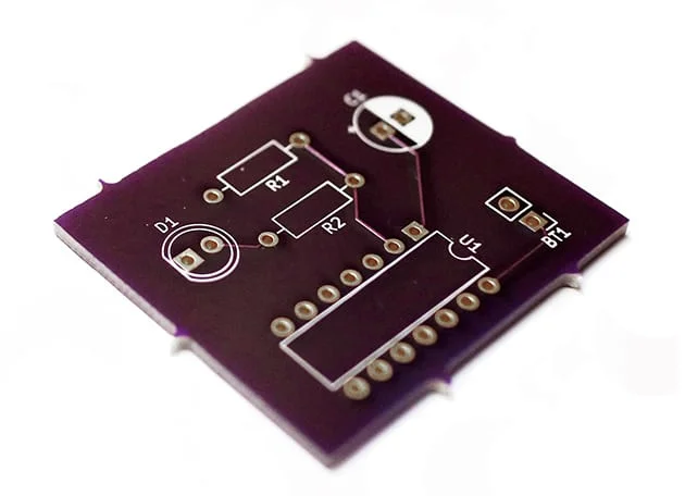
PCB designing (Printed Circuit Board designing) is the process of translating a circuit schematic into a physical layout that can be manufactured and assembled. It involves strategic placement of components, routing of copper traces, and layering of conductive and insulating materials — all while ensuring electrical performance, advanced printed circuit technology, and manufacturability.
Key stages in PCB designing and flexible PCB manufacturing include:
Logical design of circuit components and connections
Precise arrangement of components and routing paths.
Verification against manufacturing constraints.
Output files used for PCB fabrication.
| Specification | Details |
|---|---|
| Layers | 1 to 20 |
| Board Type | Rigid, Flex, Rigid-Flex |
| Trace Width/Spacing | As low as 3 mils |
| Impedance Control | Supported |
| Surface Finish | HASL, ENIG, OSP, Immersion Silver |
Experience the perfect blend of reliability and precision with our high-performance _PCB designing_, _flexible PCB manufacturing_, and _advanced printed circuit technology_ solutions.
| Feature | Cutek Circuits | Standard Designers |
|---|---|---|
| Signal Integrity | Optimized for high-speed & EMI | Basic routing |
| Customization | Full stack design-to-manufacture | Limited integration |
| Prototyping Speed | 3–5 days for small boards | 7–10 days |
| Compliance | IPC & RoHS certified | Varies |
| Design Review | Multi-point checks & simulations | Minimal validation |
Rigorous quality checks and industry-standard certifications ensure every PCB meets the highest performance and reliability standards:
Our standard turnaround time is 3–5 working days for prototype designs. Complex or multilayer boards may take slightly longer depending on requirements.
Yes, we specialize in high-speed digital and RF PCB designs with impedance control, signal integrity optimization, and EMI/EMC compliance.
Absolutely. All our PCB layouts undergo thorough DFM and DFT checks to ensure ease of manufacturing and post-production testing.
Yes, we offer full BOM preparation and can support component selection and sourcing to match your budget and lead time.
You'll receive Gerber files, drill files, BOM, pick-and-place files, and 3D models — everything needed for fabrication and assembly.
Yes, we design multilayer PCBs with up to 20+ layers, optimized for signal integrity, power distribution, and compact form factors in complex applications.
At CuteK Circuits, we combine cutting-edge technology, customization flexibility, and competitive pricing to deliver the best keyboards for your needs.
We specialize in PCB designing, offering reliable solutions for custom applications. Our capabilities also include flexible PCB manufacturing, ensuring durability and adaptability in compact electronic systems.
We leverage advanced printed circuit technology to meet the highest industry standards and performance expectations.
Fill out the form and our team will get back to you.
Fill out the form now and our team will get back to you shortly with the perfect solution tailored to your needs.
Quick response. Expert support.