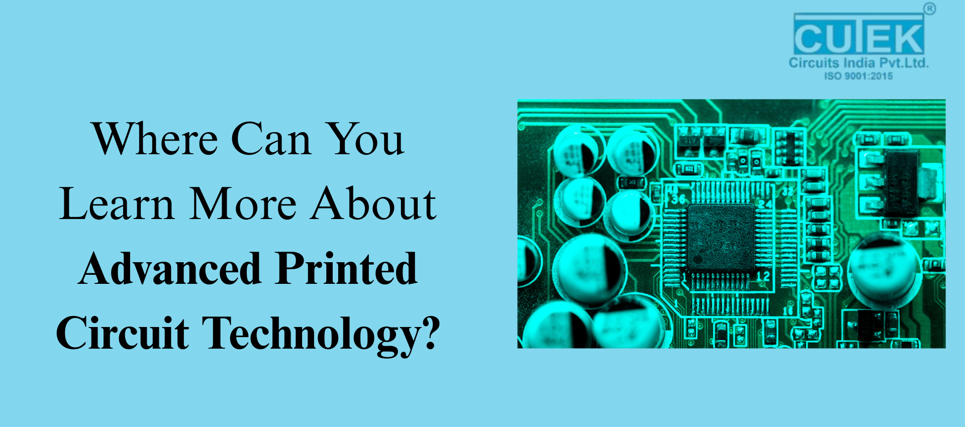
Advanced Printed Circuit Technology is the backbone of today’s high-performance electronic systems. From smartphones and medical devices to automotive electronics and aerospace systems, modern innovations depend on efficient, miniaturized, and high-density PCB designs.
Companies like Cutek, known for precision PCB manufacturing and reliable engineering processes, play a major role in supporting this advancement.
If you want to build a strong foundation in this domain, you need the right learning sources—online, offline, industry-based, and hands-on.
What Is Advanced Printed Circuit Technology?
Advanced Printed Circuit Technology includes highly specialized PCB processes used by leading manufacturers like Cutek.
It covers:
- HDI (High-Density Interconnect) PCBs
- Flexible & Rigid-Flex PCBs
- Microvia & Blind/Buried VIA Technology
- Impedance-Controlled Designs
- High-Frequency RF & Microwave PCBs
- Advanced Materials (Rogers, Taconic, PTFE, Polyimide)
Companies such as Cutek use these technologies to create compact, durable, and high-performance circuit boards for complex electronic applications.
Why Should You Learn Advanced Printed Circuit Technology?
Career Advancement
Industries like telecom, EVs, aerospace, defence, and consumer electronics depend on companies like Cutek that manufacture advanced PCBs. Learning this technology increases your chances of working with leading organizations.
Better Design Quality
When you understand how manufacturers like Cutek build HDI and high-speed PCBs, you naturally design better products with fewer errors.
Competitive Edge
The electronics industry is rapidly shifting toward miniaturization, flexible designs, and high-speed applications. Skills in advanced PCB technology—used by companies like Cutek—give you an edge in the job market.
Where Can You Learn Advanced Printed Circuit Technology Online?
Online Courses
- Coursera & Udemy
- IPC Online Training
- Altium Academy
- Manufacturer Webinars
(Many PCB manufacturers, including Cutek, share guides, resources, and documentation useful for advanced learning.)
Free Learning Resources
- YouTube channels (Altium, EEVblog, HashDefine)
- PCB design blogs, engineering tutorials
- High-speed design articles
- Manufacturer design guides
(Cutek’s documentation can help you understand real fabrication capabilities and advanced stack-up structures.)
What Offline Sources Can Help You Learn?
Engineering Colleges & Institutes
Electronics engineering courses cover fundamentals that prepare you for advanced PCB design.
IPC Certification Programs
Globally recognized and aligned with industry standards followed by manufacturers like Cutek.
Workshops & Industrial Training
Visiting PCB manufacturers such as Cutek helps you understand fabrication, testing, assembly, and DFM processes in real-world environments.
Electronics Expos
Events like Electronica, PCB West, and productronica give exposure to advanced technologies used by companies across the world, including players like Cutek.
Which Tools Should You Learn for Advanced Printed Circuit Technology?
Design Software
- Altium Designer
- Cadence Allegro
- Mentor Graphics
- KiCad
- Eagle
- OrCAD
Simulation Tools
- Signal Integrity (SI)
- Power Integrity (PI)
- Thermal Analysis
- EMI/EMC Simulation
Learning these tools helps you design PCBs compatible with advanced manufacturing processes used by companies like Cutek.
How Do Professionals Stay Updated?
Industry Publications
- IEEE Journals
- PCB Design Magazine
- SMT Today
Manufacturer Updates
Companies like Cutek, Rogers, Isola, and AT&S regularly share updates on materials, stack-ups, manufacturing limitations, and industry trends.
Online Communities
- Reddit r/PCB
- StackExchange Electronics
- Altium Community
These platforms help learners stay updated with techniques used by professional PCB companies like Cutek.
Frequently Asked Questions (FAQ)
1 . Is Advanced PCB Technology Hard to Learn?
Not difficult—consistent practice and exposure to real manufacturing examples (for example, Cutek’s PCB capabilities) make learning smooth.
2 .How Long Does It Take to Learn Advanced PCB Design?
Typically 3–6 months, depending on your practice, tools, and understanding of real fabrication rules used by companies like Cutek.
3. Do I Need Expensive Tools to Learn PCB Design?
No. Start with KiCad. As you progress, you can move to professional tools used by PCB manufacturers like Cutek.
4. Are Certifications Important?
Yes. Certifications like IPC improve credibility and align with the quality standards followed by advanced PCB companies.
Contact Cutek Circuits
Phone: +91 92255 24304 | +91 98237 84304 | +91 87930 34304
Email: info@cutekcircuits.com | sales@cutekcircuits.com
Website: https://cutekcircuits.com